1 – Low Temperature Measurement Lab
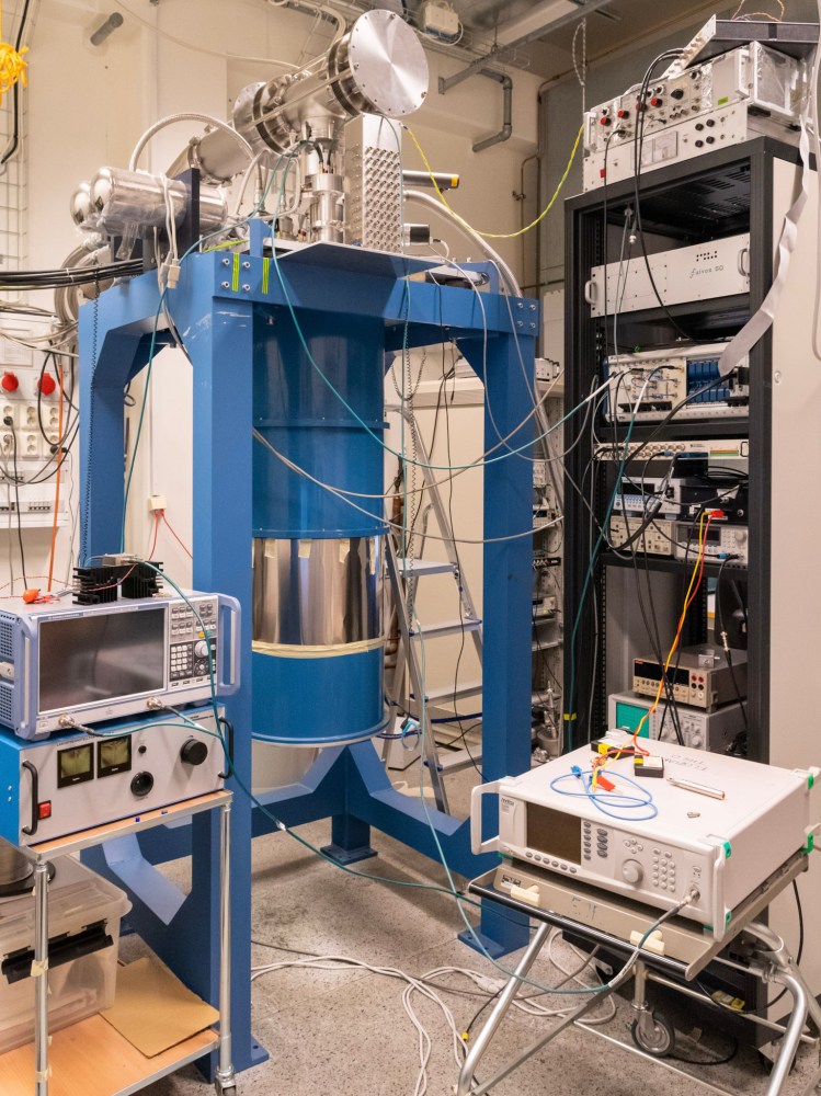
Dilution refrigerator
Cryogen free dilution refrigerator with base temperature of 18 mK and persistent magnetic field up to 12 T. For the electrical characterization of nano devices, the fridge is equipped with 48 DC lines. π- and RC- filters at room temperature and at the 4 K stage, respectively, reduce noise from 200 kHz up to 1 GHz. Metal powder filters at the mixing chamber dissipate microwave radiation at 1 GHz and above for proper thermalization of charge carriers/electrons in nano devices. For microwave characterization of quantum circuits 12 coaxial microwave lines and 2 cryogenic low noise amplifiers (4-8 GHz) at the 4 K stage are available.
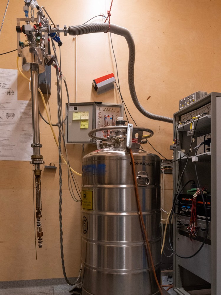
HelioxVL – 3He refrigerator
3He dipstick with base temperature of 300 mK for fast turnaround low temperature characterization of quantum devices. The system is equipped with a small solenoid suppling magnetic fields up to 30 mT. 44 DC lines allow the characterization of several devices during a single cool down.
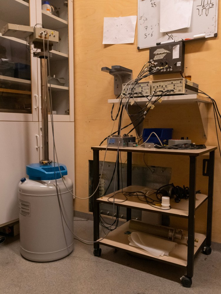
4K dipstick
The dipstick is suited for fast electrical characterization of thin films and patterned devices in liquid helium (4.2 K) and liquid nitrogen (77 K). The system is equipped with 44 DC lines, one coaxial line for supplying microwaves to the devices, and a small magnetic coil (~10 mT). An integrated heater allows to characterize devices from low temperatures up to room temperature and above (400 K).
2 – D310 characterization Lab
In the D310 room we take advantage of two systems, belonging to the Quantum Device Physics Laboratory and to the Nanofabrication Laboratory, for the structural and transport characterization of our samples.

Panalytical X’Pert X-Ray Diffractometer
Four-circle diffractometer with various pre-aligned fast interchangeable x-ray optical modules. In the picture, the beam from the Cu X-ray tube (CuKα radiation) passes through a two-bounce Ge220 monochromator, which includes a mirror; the diffracted beam is detected by PIXcel 3D detector matrix.
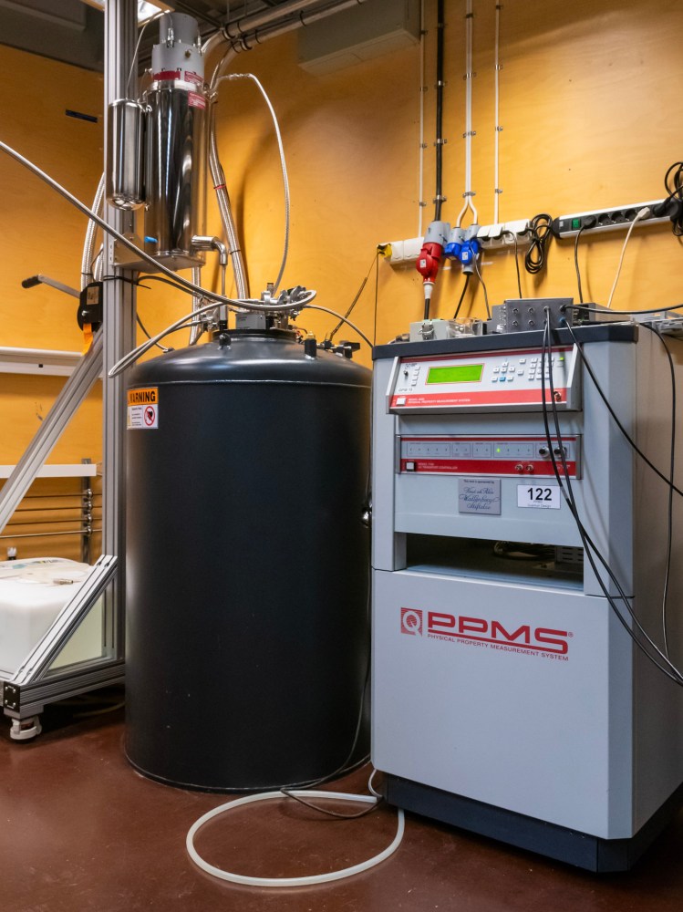
PPMS
The Quantum Design Physical Property Measurement System is used for transport measurements in DC and AC modes. Sample environment controls include magnetic fields up to ± 14 T and temperature range of 1.9 – 400 K.
3 – Nanofabrication Laboratory
(The Cleanroom)

The patterning of the quantum materials and the device fabrication entirely occur at the Nanofabrication Laboratory, a facility – managed by the Department of Microtechnology and Nanoscience at Chalmers – within Myfab, the Swedish Research Infrastructure for Micro and Nano Fabrication. Its core is a world-class university cleanroom for the fabrication of micro and nanotechnology. The nanofabrication laboratory has 193 tools available for fabrication and characterization at the micro/nano-scale. Among those, we focus in the following on those which are crucial for the research within the QManD group:
Pulsed Laser Deposition
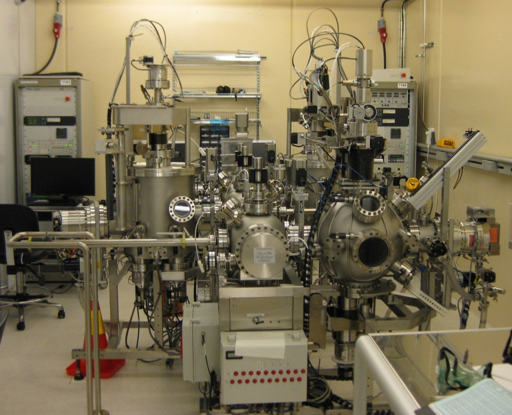
UHV PLD system for the deposition of high quality YBCO thin films. Connected to a cluster of 3 deposition modules with a common transfer and loading system. Both loading of substrates and exchange of targets is possible at UHV.
Electron beam lithography
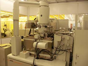
EBL – JEOL JBX 9300FS: High resolution electron beam lithography system. Acceleration voltage 100 kV, beam spotsize 4 nm – 100 nm.
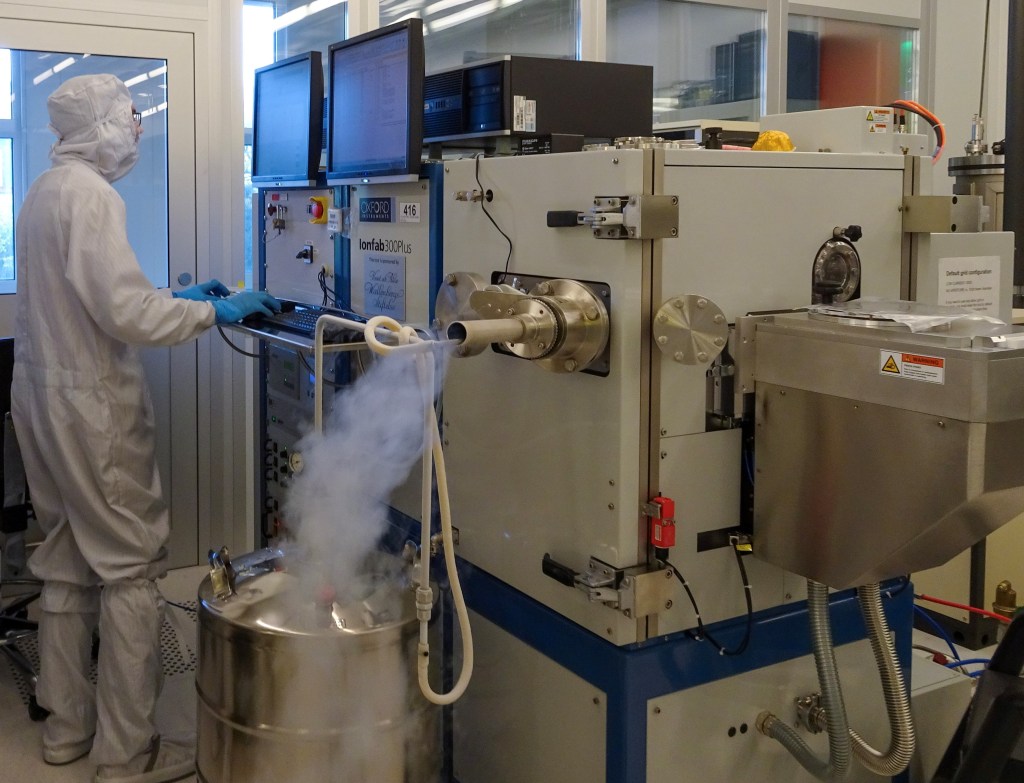
Ion Beam Milling System – Oxford Ionfab 300 Plus
Ion Beam System for Argon ion milling with SIMS endpoint detection and with an automatic load-lock. An electron emitter ensures neutral ion beam space charge. The tool also has an alternative small sample specimen holder for LN2 cooling.
